
�������: 1-11 ���鵽�����ӿ�ѧ�뼼�� Advances����ؼ�¼11�� . ��ѯʱ��(0.062 ��)

�Ϸ��Ƽ���ѧ��Էݼ/���������ѧ֣�ӽ��Ŷ�Science Advances������֯�ﵥƬ���ɵ����߱�Ƥ���ﴫ�����������о���չ��ͼ��
��Էݼ ֣�ӽ� Science Advances ֯�ﵥƬ ���ﴫ�� �ɴ��� ��������
2023/11/29
���գ��Ϸ��Ƽ���ѧ��Էݼ�����������������ѧ֣�ӽ������������Կɴ���������������ȡ���о���չ������о��ԡ�A Monolithically Integrated In-textile Wristband for Wireless Epidermal Biosensing���ڹ��ʶ����ڿ�Science Advances�Ϸ������Ͽƴ�-������2021�����ʿ����С��Ϊ���ĵ�һ���ߣ���Էݼ���Ϸ��Ƽ���...

New blue light technique could enable advances in understanding nanoscale technologies��ͼ��
���⼼�� �������� �뵼�� ���Ӳ�Ʒ
2023/6/26
A team of Brown University researchers created a solution to a nanoscale resolution challenge that has for decades limited the study of materials that could lead to more energy efficient semiconductor...

ȫ����л�����ѧ�ؼ����ϡ�����Science Advances��������ѧκ����Ŷ��з��뵼���Թ�̽���ͼ��
ȫ��� �л�����ѧ���� �뵼���Թ�̽�
2022/7/1
�����һ�ָ߾������켼�����㷺Ӧ���ڰ뵼����ҵ�����ڹ�̵Ĺ���������칤���Ѵﵽ5�������ڵ㣬����оƬ�Ͼ���������Ѵ���ڼ������֮�£�������Һ���ӹ����л�����ѧ�ͻ�ԶԶ����ڹ������ѧ������ӡˢ�л���·�ľ�����ܶ�����ֻ��60 units cm-2��ͨ����̼ӹ��л���·���в��������л��뵼�塢����ʺ͵��壩��ȫ��̹��շ����������ƽ��л�����ѧ�ͻ����ܶȼ��ɵ���Ч�ֶΡ�
Science Advances����������ѧ���Ӳ��Ͽ�ѧ���ĺ�ΰ��л�ij������������������Ҫ��չ��ͼ��
Science Advances ������ѧ ���Ӳ��Ͽ�ѧ ��ΰ л�ij� ��������̬
2018/5/11
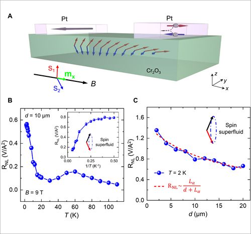
�����������ѧ���Ӳ������ĺ�ΰ��л�ijε���ɵ��о��Ŷ��ڹ������״γɹ���ʵ���Ϲ۲������������̬����Ҫʵ��֤�ݣ����������������һ���ش�ͻ���Խ�չ���о�С���������ü�����������Ӽ��������˾���ԭ�Ӽ���ƽ���ȵķ�����Cr2O3��Ĥ���ǵ�ɵľ�Ե�塣���÷Ǿ����������˵ļ��������ȷ����ڲ��缫��Cr2O3��Ĥ����ע������������������ѹ��������һ�����缫�����ò�����������ЧӦ���������������ˣ�ͼA����ʵ...
���ӿƼ���ѧ���������Ŷ���Science�ӿ�Science Advances�Ϸ������гɹ���ͼ��
���ӿƼ���ѧ ���������Ŷ� Science�ӿ� Science Advances ���� �������ѧ
2017/7/7
2017��6��2�գ����ӿƼ���ѧ���ӱ�Ĥ�뼯�����������ص�ʵ���ҡ�������������ѧԺ���������Ŷ���Science�ӿ���Science Advances���Ϸ�����Ϊ��Ultralight, scalable, and high-temperature�Cresilient ceramic nanofiber sponges�����о����ġ����ӿƼ���ѧ���ӱ�Ĥ�뼯�����������ص�ʵ����Ϊ��һ������λ������...
2017 SPIE X���ߺ�EUV��ѧ����ѧ��չר����飨Advances in Metrology for X-Ray and EUV Optics VII��
2017 SPIE X���� EUV��ѧ����ѧ��չ ר�����
2017/4/25
Conference Sessions:1: At-Wavelength Metrology ;2: Metrology of VLS Gratings Technology Hot Topics: How Optics and Photonics Drive Innovation ;3: Calibration and Nanoradian Metrology ;4: Metrology Fac...
New technology using silver may hold key to electronics advances
silver may hold key electronics advances
2015/7/13
Engineers at Oregon State University have invented a way to fabricate silver, a highly conductive metal, for printed electronics that are produced at room temperature.There may be broad applications i...
Recent Advances in Perfectly Matched Layers in Finite Element Applications
Finite element method (FEM) perfectly matched layer (PML) locally-conformal PML
2009/7/28
We present a comparative evaluation of two novel and practical perfectly matched layer (PML) implementations to the problem of mesh truncation in the finite element method (FEM): locally-conformal PML...
Advances in DWDM Optical Networking Technology
DWDM optical networks OADM OXC IP/DWDM all-optical metropolitan selfhealing
2010/7/15
Wavelength routed Optical networking technology is the certain technology for future transport network upgrading because of its potential cost-effectiveness, large capacity, flexible reconfiguration a...
Advances in Electrode Materials Research
Electrode Materials the microelectronics industry
2010/12/14
The technologies of primary (non-rechargeable) and secondary (rechargeable)
lithium batteries have been developed in parallel to the developments in the
microelectronics industry for about 20 years....
Advances in Low Cost Silver-Containing Thick Film Conductors
Silver-Containing Thick Film Conductors resistor networks hybrid integrated circuits
2010/12/28
Extensive use of thick film materials to manufacture resistor networks and hybrid integrated circuits has come about because of economic, processing and functional advantages over other technologies i...
�й��о����������а�-��
- ���ڼ���...
�й�ѧ���ڿ����а�-��
- ���ڼ���...
�����ѧ���л������а�-��
- ���ڼ���...
�й���ѧ���а�-��
- ���ڼ���...
�ˡ���-ƪ
- ���ڼ���...
�Ρ���-ƪ
- ���ڼ���...
��������-ƪ
- ���ڼ���...
�������� -ƪ
- ���ڼ���...
֪ʶҪ��-ƪ
- ���ڼ���...
���ʶ�̬-ƪ
- ���ڼ���...
��������-ƪ
- ���ڼ���...
ѧ��ָ��-ƪ
- ���ڼ���...
ѧ��վ��-ƪ
- ���ڼ���...