
�������: 106-120 ���鵽�����ʶ�̬ �뵼�弼������ؼ�¼216�� . ��ѯʱ��(3.445 ��)
Electronics get a power boost with the addition of a simple material
Electronics power boost simple material
2015/11/12
The tiny transistor is the heart of the electronics revolution, and Penn State materials scientists have just discovered a way to give this workhorse a big boost, using a new technique to incorporate ...
Individual transistors made from carbon nanotubes are faster and more energy efficient than those made from other materials. Going from a single transistor to an integrated circuit full of transistors...
�¹�������в���ŷ��ίԱ����ظ������ڽ��չ�ͬ������ŷ���о���Ŀ������������(SeNaTe)������Ŀּ�ڿ�����С�������յļ��ɵ�·���Ӷ���������оƬ�ļ������������Կ�ѧ���ҵ���42��ŷ��鹲ͬ�����������ɵ�·�Ľṹ�ߴ���С��Ŀǰ���оƬ�ߴ��һ�롣
Under the direction of Latha Venkataraman, associate professor of applied physics at Columbia Engineering, researchers have designed a new technique to create a single-molecule diode, and, in doing so...
In 2013 James Hone, Wang Fong-Jen Professor of Mechanical Engineering at Columbia Engineering, and colleagues at Columbia demonstrated that they could dramatically improve the performance of graphene��...

������ѧ���������������˱�(��Ϊ����ԭ�Ӻ�)�İ뵼�壬�����һ�����������������䲻����Ч���ߣ����������ҿ���Ŀǰ�ĵ����豸���ݡ��о���Ա��ʾ����һ�о��ɹ�Ϊ����������ù���ǵ��Ӵ�����Ϣ����һ�������豸�춨�˼�ʵ�Ļ�������ҽ�Ƶ������и��ٵ����Ӳ�Ʒ���������������а�����Ҫ��ɫ����Ϊ�������ִ����㡢ͨѶ������ʹ���Ҫ��ѧ����һֱϣ�������������С�Һ��ܸ��͵ļ���ϵͳ����ʢ�ٴ�ѧ��˹̹����ѧЯ...
Beyond silicon: New semiconductor moves spintronics toward reality��ͼ��
Beyond silicon New semiconductor spintronics
2015/3/4
A new semiconductor compound is bringing fresh momentum to the field of spintronics, an emerging breed of computing device that may lead to smaller, faster, less power-hungry electronics.Created from ...
It��s nearly 50 years since Gordon Moore predicted that the density of transistors on an integrated circuit would double every two years. ��Moore��s Law�� has turned out to be a self-fulfilling prophecy t...

Stacking Two-Dimensional Materials May Lower Cost of Semiconductor Devices��ͼ��
Two-Dimensional Materials Lower Cost Semiconductor Devices
2014/12/30
Semiconductor heterostructures provide a powerful platform to engineer the dynamics of excitons for fundamental and applied interests. However, the functionality of conventional semiconductor heterost...

Researchers find new way to move atomically thin semiconductors for use in extremely flexible devices��ͼ��
thin semiconductors flexible devices
2014/12/1
Researchers from North Carolina State University have developed a new way to transfer thin semiconductor films, which are only one atom thick, onto arbitrary substrates, paving the way for flexible co...
Protecting our processors
semiconductor security
2014/10/9
The National Science Foundation (NSF) and Semiconductor Research Corporation (SRC) today announced nine research awards to 10 universities totaling nearly $4 million under a joint program focused on S...

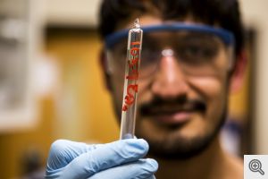
UCSB researchers develop ultrasensitive biosensor from molybdenite semiconductor��ͼ��
ultrasensitive biosensor molybdenite semiconductor
2014/9/12
Move over, graphene. An atomically thin, two-dimensional, ultrasensitive semiconductor material for biosensing developed by researchers at UC Santa Barbara promises to push the boundaries of biosensin...
�����������ߵ������л�����
���� �ߵ����� �л����� �뵼��
2014/8/25
�����л����Ͼ����������뵼�壬�����л���������ܺ��л�����ܵȣ���ӵ�������һ���ĸߵ����Ե��л�������Ȼ�dz�ϡ�١��л������з�������ڵ�һ�������ǣ����õĵ�������Ҫ����Ͼ��кܸߵĽᾧ�ȣ�������ṹȴ�����ڲ��ϵļӹ��ͳ��͡����ڣ�����˹����˹����ѧ���о��Ŷӿ�����һ���µ��л����ϣ����������Ըߣ����ҷdz��������е��ԣ��ɹ��˷����������⡣
�������й��о���Ա2014��5��5�������������ҿ�ѧԺѧ�����ϱ���˵�����ǿ�����һ�ֻ��ڰ뵼��оƬ�����ǵ�����ǰ��Ϸ��������Ը����и�Ѫ������̥���Ƿ������ۺ�������Ⱦɫ���쳣�йص�����ȱ�ݡ�
New 'tunable' semiconductors will allow better detectors, solar cells
New 'tunable' semiconductors allow better detectors solar cells
2014/4/16
One of the great problems in physics is the detection of electromagnetic radiation �C that is, light �C which lies outside the small range of wavelengths that the human eye can see. Think X-rays, for ex...
�й��о����������а�-��
- ���ڼ���...
�й�ѧ���ڿ����а�-��
- ���ڼ���...
�����ѧ���л������а�-��
- ���ڼ���...
�й���ѧ���а�-��
- ���ڼ���...
�ˡ���-ƪ
- ���ڼ���...
�Ρ���-ƪ
- ���ڼ���...
��������-ƪ
- ���ڼ���...
�������� -ƪ
- ���ڼ���...
֪ʶҪ��-ƪ
- ���ڼ���...
���ʶ�̬-ƪ
- ���ڼ���...
��������-ƪ
- ���ڼ���...
ѧ��ָ��-ƪ
- ���ڼ���...
ѧ��վ��-ƪ
- ���ڼ���...